Tag: TI

Following the kernel #4 – MLO part 1

We have finished last period on jumping into reset vector of the MLO code. If you haven’t done it yet, I encourage you to clone U-Boot repository from GitHub https://github.com/u-boot/u-boot. I’m working on the newest master commit a6ba59583abd4085db5ab00358d751f175e2a451. As I wrote, U-Boot is configured via KBuild with default am335x set.

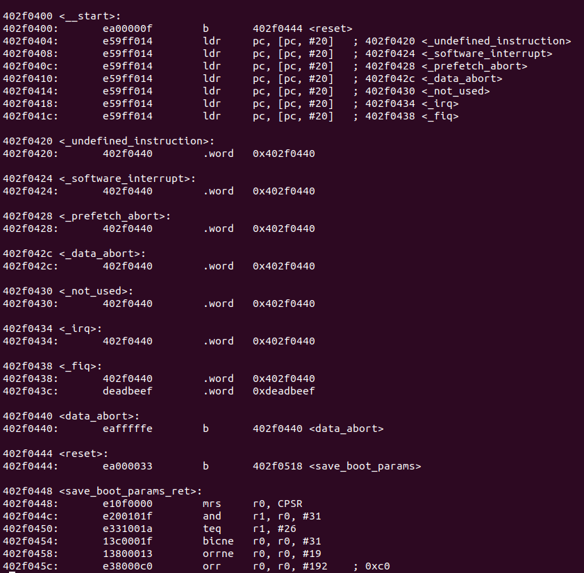
Reset vectors of MLO are defined in common for U-Boot and MLO (TPL and SPL) place – arch/arm/lib/vectors.S file. If you were careful enough, your debugger should stop on the line 87:

/*
 *************************************************************************
 *
 * Exception vectors as described in ARM reference manuals
 *
 * Uses indirect branch to allow reaching handlers anywhere in memory.
 *
 *************************************************************************
 */

_start:
#ifdef CONFIG_SYS_DV_NOR_BOOT_CFG
	.word	CONFIG_SYS_DV_NOR_BOOT_CFG
#endif
	ARM_VECTORS // <--- right here
#endif /* !defined(CONFIG_ENABLE_ARM_SOC_BOOT0_HOOK) */

ARM_VECTORS is the macro defined few lines above (21-34).

/*
 * A macro to allow insertion of an ARM exception vector either
 * for the non-boot0 case or by a boot0-header.
 */
        .macro ARM_VECTORS
#ifdef CONFIG_ARCH_K3
	ldr     pc, _reset
#else
	b	reset
#endif
	ldr	pc, _undefined_instruction
	ldr	pc, _software_interrupt
	ldr	pc, _prefetch_abort
	ldr	pc, _data_abort
	ldr	pc, _not_used
	ldr	pc, _irq
	ldr	pc, _fiq
	.endm

Our architecture is OMAP2+ (CONFIG_ARCH_OMAP2PLUS – check it with make menuconfig for practice), so our code includes b reset part, and this is the instruction placed under our first breakpoint. We are jumping into the reset routine. This one is defined in arch/arm/cpu/armv7/start.S file. Reset routine starts in line 38.

reset:
	/* Allow the board to save important registers */
	b	save_boot_params
save_boot_params_ret:
#ifdef CONFIG_ARMV7_LPAE
/*
 * check for Hypervisor support
 */
	mrc	p15, 0, r0, c0, c1, 1		@ read ID_PFR1
	and	r0, r0, #CPUID_ARM_VIRT_MASK	@ mask virtualization bits
	cmp	r0, #(1 << CPUID_ARM_VIRT_SHIFT)
	beq	switch_to_hypervisor
switch_to_hypervisor_ret:
#endif
	/*
	 * disable interrupts (FIQ and IRQ), also set the cpu to SVC32 mode,
	 * except if in HYP mode already
	 */
	mrs	r0, cpsr
	and	r1, r0, #0x1f		@ mask mode bits
	teq	r1, #0x1a		@ test for HYP mode
	bicne	r0, r0, #0x1f		@ clear all mode bits
	orrne	r0, r0, #0x13		@ set SVC mode
	orr	r0, r0, #0xc0		@ disable FIQ and IRQ
	msr	cpsr,r0

/*
 * Setup vector:
 * (OMAP4 spl TEXT_BASE is not 32 byte aligned.
 * Continue to use ROM code vector only in OMAP4 spl)
 */
#if !(defined(CONFIG_OMAP44XX) && defined(CONFIG_SPL_BUILD))
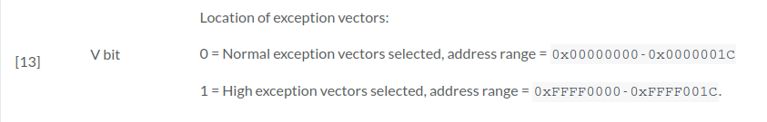
	/* Set V=0 in CP15 SCTLR register - for VBAR to point to vector */
	mrc	p15, 0, r0, c1, c0, 0	@ Read CP15 SCTLR Register
	bic	r0, #CR_V		@ V = 0
	mcr	p15, 0, r0, c1, c0, 0	@ Write CP15 SCTLR Register

#ifdef CONFIG_HAS_VBAR
	/* Set vector address in CP15 VBAR register */
	ldr	r0, =_start
	mcr	p15, 0, r0, c12, c0, 0	@Set VBAR
#endif
#endif

	/* the mask ROM code should have PLL and others stable */
#ifndef CONFIG_SKIP_LOWLEVEL_INIT
#ifdef CONFIG_CPU_V7A
	bl	cpu_init_cp15
#endif
#ifndef CONFIG_SKIP_LOWLEVEL_INIT_ONLY
	bl	cpu_init_crit
#endif
#endif

	bl	_main

As we can see, here we have more code to focus on. This code prepares CPU before execution and call _main function at last stage. First thing is jumping into save_boot_params routine. This one is defined in arch/arm/mach-omap2/lowlevel_init.S.

ENTRY(save_boot_params)
	ldr	r1, =OMAP_SRAM_SCRATCH_BOOT_PARAMS
	str	r0, [r1]
	b	save_boot_params_ret
ENDPROC(save_boot_params)

Do you remember part 1 of this series? One of the last thing done by the ROM Code is passing boot device information via pointer passed to r0 register, just before running MLO. As we can see, this pointer is stored under OMAP_SRAM_SCRATCH_BOOT_PARAMS address. r0 for sure will be utilized later, so this is the first thing done. After that, flow is going back to rest of reset.

CONFIG_ARMV7_LPAE is turned off, so we are going to line 56. The Current Program State Register is set. If processor is in Hypervisor Mode it is left unchanged, otherwise Supervisor mode is set. After that all interrupts are masked with that register, no matter which mode is running. Supervisor mode (SVC) is state of processor proper for running kernel mode, this is worth noting. If you want to learn more about ARM processor modes, examine Reference Manual of ARMv7 architecture.

Right after that more sophisticated things are done. MCR and MRC instructions are used. These are instructions communicating with coprocessors attached on the silicon. There are maximum 16 coprocessors – p15 is so called Control Processor , described here https://developer.arm.com/documentation/ddi0360/e/control-coprocessor-cp15/about-control-coprocessor-cp15?lang=en. Instruction mnemonics supported by it are extensively described here https://developer.arm.com/documentation/ddi0360/e/control-coprocessor-cp15/summary-of-cp15-instructions. These sites refer to not our architecture – some things might be not the same as in our chip, but they are well explained.

As you could read in above links, first instruction mrc p15, 0, r0, c1, c0, 0 loads current value of MMU-related Control Register into local, core register r0. Then program clears V-bit (with bic instruction), which means, that exception vectors are kept in 0x00000000 address range and write it back to the Control Register with mcr.

Next instruction mcr p15, 0, r0, c12, c0, 0 sets the Vector Base Address Register inside Control Processor to the address of _start. This symbol was defined in our first listing in this article. Now all the exceptions caught by processor should be handled by the Vector defined in MLO (described in vector.s).

Before we jump to the long-awaited C code there are couple of assembly routines which must be executed. The first one is cpu_init_cp15. This one is defined in file arch/arm/cpu/armv7/start.S, line 143. As you can see, there are a lot of MCR transfers, I will try to explain general idea behind the whole procedure without analyzing every single mnemonic.

The name of routine tells us, that once again coprocessor number 15 will be initialized. As the comments says line 143-148 invalidates all data saved in L1 cache, which after restart may have wrong values. These are TLBs (Translation Lookaside Buffers – records which speed up resolving virtual address into physical memory), instruction caches which might buffer adjacent blocks of assembly code, to speed up instruction fetches, and lastly invalidation of BP (Branch Prediction) arrays is done. Branch prediction is another mechanism of speeding up pipeline processors to fetch the right instruction, even if it is not the next mnemonic of our assembly code. If you want learn more in this area, I encourage to read wiki article https://en.wikipedia.org/wiki/Branch_predictor.

After invalidating caches, Data Synchronization Barrier is done to explicitly wait for the end of all memory operations, and ISB (Instruction Synchronization Barrier), described in documentation as flushing prefetch buffer is done. As documentation says:

The Flush Prefetch Buffer instruction flushes the pipeline in the processor, so that all instructions following the pipeline flush are fetched from memory, (including the instruction cache), after the instruction has been completed. Combined with Data Synchronization Barrier, and potentially a memory barrier, this ensures that any instructions written by the processor are executed. This guarantee is required as part of the mechanism for handling self-modifying code. The execution of a Data Synchronization Barrier instruction and the invalidation of the Instruction Cache and Branch Target Cache are also required for the handling of self-modifying code. The Flush Prefetch Buffer is guaranteed to perform this function, while alternative methods of performing the same task, such as a branch instruction, can be optimized in the hardware to avoid the pipeline flush (for example, by using a branch predictor).

Next bunch of assembly is commented as disabling MMU stuff and caches. Once again c1,c0 operation (Read Control Register) is made, than V-bit (once again), and CAM bits are cleared. Then A (bit 1) and Z (bit 11) are set. V-bit was described, previously. I don’t know why it’s repeated. CAM bits (https://developer.arm.com/documentation/ddi0360/e/control-coprocessor-cp15/register-descriptions/c1–control-register?lang=en) disables data Cache, Alignment fault checking and MMU. According to the hash-defines, we can turn on or turn off instruction cache in this place. In our configuration it is turned on, so setting bit with orr instruction is made.

After that, bunch of Errata stuff is done. Fortunately, none of these are applied in our build beside CONFIG_ARM_CORTEX_A8_CVE_2017_5715. But before that more interesting operations are done

	mov	r5, lr			@ Store my Caller
	mrc	p15, 0, r1, c0, c0, 0	@ r1 has Read Main ID Register (MIDR)
	mov	r3, r1, lsr #20		@ get variant field
	and	r3, r3, #0xf		@ r3 has CPU variant
	and	r4, r1, #0xf		@ r4 has CPU revision
	mov	r2, r3, lsl #4		@ shift variant field for combined value
	orr	r2, r4, r2		@ r2 has combined CPU variant + revision

/* Early stack for ERRATA that needs into call C code */
#if defined(CONFIG_SPL_BUILD) && defined(CONFIG_SPL_STACK)
	ldr	r0, =(CONFIG_SPL_STACK)
#else
	ldr	r0, =(CONFIG_SYS_INIT_SP_ADDR)
#endif
	bic	r0, r0, #7	/* 8-byte alignment for ABI compliance */
	mov	sp, r0

Once again CP15 is used to read our silicon ID. CPU variant and revision is combined and stored in r2 register. After that, according to configuration stack pointer address is chosen – in our case it is 0x4030ff10 (the value of CONFIG_SYS_INIT_SP_ADDR). Check this address in part #1 of my series. You will find out, that it’s one of the highest accessible address on Internal SRAM memory. This address is aligned to 8-bytes with clearing 3 least significant bits. Finally stack pointer is initialized with movopcode. Wohoo! Doing it is last thing prepared by cpu_init_cp15 routine, so we are going back to the reset routine and jump to another place, called cpu_init_crit.

ENTRY(cpu_init_crit)
	/*
	 * Jump to board specific initialization...
	 * The Mask ROM will have already initialized
	 * basic memory. Go here to bump up clock rate and handle
	 * wake up conditions.
	 */
	b	lowlevel_init		@ go setup pll,mux,memory
ENDPROC(cpu_init_crit)

It is the place, where more specialized initialization might be done. Our lowlevel_init procedure is implemented in arch/arm/cpu/armv7/lowlevel_init.S

WEAK(s_init)
	bx	lr
ENDPROC(s_init)
.popsection

.pushsection .text.lowlevel_init, "ax"
WEAK(lowlevel_init)
	/*
	 * Setup a temporary stack. Global data is not available yet.
	 */
#if defined(CONFIG_SPL_BUILD) && defined(CONFIG_SPL_STACK)
	ldr	sp, =CONFIG_SPL_STACK
#else
	ldr	sp, =CONFIG_SYS_INIT_SP_ADDR
#endif
	bic	sp, sp, #7 /* 8-byte alignment for ABI compliance */
#ifdef CONFIG_SPL_DM
	mov	r9, #0
#else
	/*
	 * Set up global data for boards that still need it. This will be
	 * removed soon.
	 */
#ifdef CONFIG_SPL_BUILD
	ldr	r9, =gdata
#else
	sub	sp, sp, #GD_SIZE
	bic	sp, sp, #7
	mov	r9, sp
#endif
#endif
	/*
	 * Save the old lr(passed in ip) and the current lr to stack
	 */
	push	{ip, lr}

	/*
	 * Call the very early init function. This should do only the
	 * absolute bare minimum to get started. It should not:
	 *
	 * - set up DRAM
	 * - use global_data
	 * - clear BSS
	 * - try to start a console
	 *
	 * For boards with SPL this should be empty since SPL can do all of
	 * this init in the SPL board_init_f() function which is called
	 * immediately after this.
	 */
	bl	s_init
	pop	{ip, pc}
ENDPROC(lowlevel_init)

arch/armv7 directory contains generic implementation of low-level init. All routines are defined as so-called weak symbols. If linker will find other with the same name, it will leave weak symbol not used and choose the other. Basically it doesn’t implement nothing new. Once again stack pointer is initialized. CONFIG_SPL_DM is defined (Driver Model for SPL), so r9 is zeroed.

Our program stack is ready, so we can use it with a pushinstruction. Link-register and instruction pointer is passed, after that branch with copying return address to link-register is done. We are jumping to s_init, but as we can see in the listing, it is empty.

Finally after returing to resetroutine, we are jumping to the _main routine, which is really, really close to the C-world. It is defined in arch/arm/lib/crt0.S. As we can see, it is the code initializing C environment (clearing BSS, preparing heap etc. We will cover it in the next part of the series.

Following the kernel #1 – ROM Code

With this article I am starting the large series, telling how precisely the Linux kernel works. Me and my readers will investigate each line of kernel code from the beginning, to a fully operable system. Hopefully, it gives us a strong foundation of Linux knowledge. I expect from you the C programming knowledge and computer architecture basics however, I will try to simplify more complicated statements, to keep less experienced readers here. As my article describes kernel code, I will frequently refer to git repository content. My suggestion is to clone the whole repo from https://git.kernel.org/pub/scm/linux/kernel/git/torvalds/linux.git and checkout to da2968ff879b9e74688cdc658f646971991d2c56 commit (the one I’m working on).

The kernel has many ports to different architectures. Telling about startup and running kernel is hard without describing whole booting process. To keep the article simple, without non-checkable abstractions I will tell you about the BeagleBone Black booting sequence. It is open-source board – schematics is right here https://github.com/beagleboard/beaglebone-black/blob/master/BBB_SCH.pdf – which contains ARM-based TI AM335x family microprocessor – AM3358. We can find its reference manual easily (https://www.ti.com/lit/ug/spruh73q/spruh73q.pdf). I will refer to these documents frequently. We have everything ready, so let’s get started.

Powering up

The story begins by powering up the device. When the voltage is turned on, PRCM (Power, Reset, and Clock Management) module detects it. This module is a central unit of power management. It decides to turn on or off voltage on electronic domains and start or stop clocking them. All the details about it are described in Chapter 8 of Reference Manual – PRCM. It includes a lot of information since this module handle functionalities such as low-power modes, different types of reset, etc. We will not cover all of them, since it is not the topic of this article. Our ARM Cortex A8 Core belongs to MPU (Microprocessor Unit) subsystem, which is quite complex and covers several Power domains – details are described in Chapter 3. For some reason, there is a split MPU power domain (Cortex A8 core, cache memories, some other modules such as IceCrusher) and Core power domain (which includes Interrupt Controller).

ROM Code

I will not cover electronic details, since it is not the essence of this article. The key point is that only the most important parts of our processor are powered up and supplied with the clock signal. Reset exception redirects CPU to non-erasable on-chip memory, written by silicon vendor (TI). As a consequence, the so-called, ROM code is started by our micro. It is the only part of the boot sequence, executed by not open-source code, but we can find a huge amount of information about it in Reference Manual and on the Internet.

Boot ROM memory offsets

Boot ROM memory is addressable directly by our micro with an 0x4000 0000 offset. All the addresses presented on the upper photo should be prefixed with 4 on the most significant digit, like in the picture below. Why they are not? During early startup, ROM may be accessed through alias address, without leading 4. So it may operate on 0x0000 0000 0x0002 BFFF space.[1]

Boot ROM entry in main memory map

Boot ROM has some advanced features, like peripheral booting or checking image signature. It needs some operational memory. At this, early-stage the only one is internal static RAM:

Internal SRAM memory map

The answer to how much of this is usable depends on the type of device. It might be GP (General-Purpose) with the secure boot features disabled, or HS (High-Secure), which do not allow to boot untrusted code. The latter of course need more operational memory during ROM Code execution.

First, 1kB is reserved on both types and could not be used. Next 109 kB (on GP) or 46 kB (on HS) is the place where the next part of the boot chain (SPL) is copied by ROM Code. The last 18 kB is general-purpose operational memory used at this stage (more info on the diagram below). For the sake of simplicity, I will cover GP device boot.

Let’s get back to the place where we begin. When our micro is powered up, it starts execution from Secure Boot ROM – maybe from address 0x0000 0000. There is not much information about this process. Only that it uses ARM TrustZone architecture to obstruct reverse engineering. We can deduce, that layout of Secure Boot ROM is similar to Public Boot ROM (own exception vectors, CRC, code, and version). We will not focus on it. The only valuable piece of information is that the first 128 kB of ROM is reserved and it is executed on the earliest startup.

ROM Code Exception Vector – reset entry

First public information is that after Secure Boot ROM execution, code jumps to public exception vector, which in turn redirects execution to Public ROM Code (0x4002 0100, aliased with 0x0002 0100). On the initialization phase, the stack is set up in Internal SRAM, ROM Code CRC is calculated, and checked against address 0x4002 0020 to detect eventual memory issues. The watchdog WDT1 is started and set up for three minutes. Exception vector base is redirected to Public Boot ROM, so any exceptions are now handled by it. Then the first configurable part is done – setting up clocks.

Clock configuration

The clocks are configured for their default values. To do this, the board creator must inform Boot ROM code, what crystal is used. It is done with hardware configuration using SYSBOOT pins.

Supported crystals and SYSBOOT pins to configure the right one

Now let’s check what crystal is placed on BeagleBone Black schematics and how SYSBOOT is configured.

OSC0 wiring
Boot configuration pins on BeagleBone Black

As we can see, the main oscillator (OSC0) is connected to a 24 MHz crystal, and as the manual says SYSBOOT pins are wired to logical 1 (14) and logical 0 (15). You may wonder why there are pull-ups and pull-downs added to the schematics on each line. I think it is to make eventual changes easier. Every pull-up has DNI annotation, which I suppose stands for Do Not Integrate. So the R80 resistor pulls down the voltage for SYSBOOT 15 pin and R56 pulls up SYSBOOT 14. R55 and R81 should not be soldered on the board.

According to these settings Public ROM code configures default clocking rates of essential devices. You can find them on the diagram below:

The peripheral clocks list is not accidental – it contains all the devices which allow chaining next parts of boot sequence – SPI memory, MMC card, UART, USB. These are a possible source of the Secondary Program Loader – which will be described in one of the next parts. (MPU_CLK sets core clocking, L3F is one of the internal silicon buses, I2C I suppose is used to check the voltage conditions. I think the EMAC clock should also be listed here).

Boot chaining

Now the Boot ROM is going to the essence of its existence. It starts searching for the next elements of the boot chain – Secondary Program Loader. It will be described in one of the next parts of this series. For now, let’s look at how ROM Code searches for it. SPL is the first program executed by chip, coming from outside the AM335x processor. The board creator must choose the right booting device list (using SYSBOOT pins), to tell ROM code, where SPL should be placed. This process is similar to setting up PC BIOS booting sequence. If one device will not contain it, the next one is taken from the list.

AM335x allows booting from memory (like MMC or internal NAND) or peripherals (UART, Ethernet, or USB). If all of the sequenced boot methods fail, ROM Code goes to one of the dead-loops (0x20080 offset). All possible SYSBOOT combinations are described in table 26-7 of Reference Manual. It is too big to paste it here, however below you can find entries, which are used on BeagleBone Black. During this series, I will use and describe external SD card boot (MMC0), to easily update new firmware and follow kernel on it :). If you want to read more about other types of boot devices, please check the Reference manual, chapter 26.

BeagleBone Black boot options

The first combination begins to boot from MMC1 (soldered 4GB embedded MMC memory). If there is no image written on eMMC, the MMC0 interface is examined, wired with the micro SD slot, which will be supplied with our SD card:

If there is no image on eMMC, then both scenarios are almost the same. We will boot from an SD card. However, if it’s not empty, we must push the uSD BOOT (S2) button, when powering up. It will pull-down the voltage on SYSBOOT 2 and force the second boot scenario – examining SPI memory (which is not attached and fails), and then the MMC0 interface. The last two options (UART/USB) are not considered, since we will supply the board with a correct image on the SD card.

MMCSD

MMCSD controller in our AM335x processor is flexible enough to handle communication with a micro SD card. There is a lot of information about MMCSD controller communication in chapter 18 of the Reference Manual. The protocol used with SD cards is quite simple. There is a clock signal (MMC0_CLK), which allows transfer through 4 data lines (MMC0_DAT0-3). Data transfers are controlled by commands, serially sent through the MMC0_CMD line. MMC0_CD is a card detection line. As you can see on the schematics, it is pulled-up to 3,3 V. If the card is inserted, mechanical switch wires this line with grounded housing, and drives this pin low. According to documentation, Boot ROM Code does not use it, but sends a command and waits for a response instead. It is reasonable, since the polarity of this signal may vary among different boards.

MMC initialization is quite complicated because it covers different standards of memory storage. MMCSD controller supports MMC memories (8 data lanes), SD cards (4, 1 DAT lane or differential transfer on UHC-II) with different size and transfer rates. The transfer might use Single Data Rate or Double Data Rate – data clocked on rising and falling edge. All these details must be figured out on the command line. The protocol used there is compatible with all standards. Data packets are sent there serially in 48-bit requests. The first two (01) creates start sequence, next 6 are the command number. Right after that, 4 bytes of argument is passed. The packet is ended with 7-bit CRC and stop bit. Command numbers are described in manuals as CMDXX, where XX is a 6-bit command number. Sometimes they are prefixed with ACMDXX, which stands for Application-Specific Command. The response might be 48 or 136-bit, depending on the request type.

MMC initialization probably starts with CMD0 – the card chip reset. I haven’t checked the sequence, however, I assume it’s safer to make sure, that card is in an idle state. In the idle state, the default 400kHz rate clocks commands and responses, which should be supported by all standards. The next command strongly depends on card type, so I will focus on SD standard. So the CMD8 is sent to determine if current voltage conditions are OK for the card. It also tells whether the card supports SD standard in version 2.0 (this command was declared there). If there is no response for it, the controller knows, that card is in an older standard.

Let’s assume, that response was correct – with the same value in the VHS field and check pattern. The next command is ACMD41. It is an Application Specific command (preceded by CMD55), which starts the initialization process. The host sends suggested configuration bits (HCS, SDXC Power Control, S18R) and check if these settings are supported by the Card. If the settings are not supported, the card goes into an Inactive state, and the whole initialization must be repeated. Otherwise, the card sends a response with OCR (Operational Conditions Register) value. It contains a busy bit that is set if card chip initialization is completed, or it is still ongoing. In that case, ACMD41 must be repeated to poll the initialization. All configuration bits are presented on the diagram below. With HCS, the host declares its support of High Capacity or eXtended Capacity conformance. If the SDXC standard is supported, Card might be put into power saving or fast mode with XPC. UHC-I standard also allows switching logic voltage to 1,8V (shorter edges and faster data transfers). It might be checked with the S18R bit and activated with CMD11 later on.

Card responds with configuration bits and current Operational Condition Register value in this format:

After this handshake, the host and card know which standard will be used during later communication (Data Transfer Mode). The next phase is Card Identification Process. All previous commands were sent in broadcast addressing, now the host must allocate an address for each card connected to the bus. To do that, it issues CMD2, as a response Card sends its Identification Number (CID). This triggers Identification State on the Card. Next CMD3 is sent by the host. As a response Card suggests a shorter Relative Card Address (RCA). If the host accepts it, in later communication card will be identified with this RCA Address. If the host does not accept it, it must repeat CMD3.

As you may notice, a card address assignment is needed. It implies, that this interface support connecting many cards on that interface. We will not go too deep into it. The important thing is that RCA is used during Data Transfer Mode, which started right after CMD3. Now we can request data read, write, or card erasure, using yielded RCA.

To do that, we must transit the card chip from the Stand-by state (in Data Transfer Mode) to the Transfer state, using CMD7. Of course, we must supply RCA argument to this request. Other cards on the bus are transitioned to a Stand-by state (if it is in Transfer mode). The whole state diagram of the Data Transfer Mode is placed below.

After triggering the CMD7 command our card is in Transfer State. By default, data transfers are made on a single DAT0 line. To extend it, we send ACMD6 request with 10b argument.

At this moment distinction between SDSC (Standard Capacity) and SDHC/XC (High Capacity/eXtended Capacity) must be made. The first group could change block length (data are sent in blocks) and could address data using bytes – but has less capacity. The latter have extended capacity, but it is always addressed using block number, which is always 512-byte sized. After this short setup, we can access our data with CMD17 (single block read) or CMD18 (multiple block read). CMD18 transfer is finished with CMD12 (stop transmission).

This state machine and read process is managed by the MMCSD driver inside ROM Code. Right above that we need some logical data structure to gather the SPL. There are several ways, we can put SPL (later named as MLO – MMC Loader) in the SD Card. The first is Raw mode – MLO is directly written on the SD Card in four copies (0x0, 0x20000, 0x40000, 0x60000 offsets), without the usage of any file system. There is also an option of writing a file called MLO in the active, FAT partition. This is the way which I will cover. In this case, FAT module handles logical memory structure.

Reference Manual presents the layered structure of ROM Code. On the top of the MMCSD driver, the FAT module is used to access data in a formatted SD Card if we use this file system.
MBR

The card can be formatted with the so-called Master Boot Record (it allows putting several partitions on the card), or whole memory may be formatted with FAT. The first approach will be used, so the first sector on our memory is a Master Boot Record (MBR). This is the logical structure, telling about partitions present on the memory and specifying their details like name or usage flags (active/not active, boot partition). The job for ROM Code is to find active FAT 12/16/32 partition with MLO file in its root folder. The structure of the MBR is presented below.

The first thing done is to recognize, if a sector is indeed MBR. To do this, the signature at the end is used. It must be equal to 0xAA55. Right after that, partition entries are examined whether any of them contains the FAT file system and it is active. There is an obvious error in the Partition End Head position – it has a 1-byte length, not 16 like on the diagram below.

This structure gives information about the placement of the partition on the SD Card. It might be written in two ways, using CHS (Cylinder Head Sector) way on 3-byte addresses (start at offset 1, end at offset 5). Or it might be specified using 4-byte LBA (Logical Block Addressing) – start at offset 8, size of the partition at offset 12. According to these data, we can check if the MBR entry is not malformed (address goes outside available memory) and move further.

FAT File System

FAT stands for File Allocation Table. It is the second logical part of this file system, after the Boot Sector, which includes BIOS Parameters Block and before Root Folder and Data Area. Boot Sector is placed on the first sector occupied by partition. Important for us is that it contains much information about file system structure:

  • Bytes per sector – in the flash drives it should be the same as block size since it is the smallest erasable piece of memory. Usually, it is equal to 512.
  • Sectors per cluster – FAT makes from whole Data Area small parts, called clusters. We could see it as the smallest allocation area. Each cluster is assigned to a single file and a single file may lay in several clusters distributed among the whole data area.
  • Position of the Root directory – it is not directly written in BIOS Parameters Block, but it may be calculated from parameters given there.
    • Number of sectors per Boot Sector
    • Number of FAT copies (to prevent data malformation FATs are usually duplicated)
    • Absolute position of the FAT partition in flash memory space

After the Boot Sector, there are File Allocation Tables. This is a register of all clusters used by a file system. The offset of the FAT cell tells, to which cluster in Data Area it is assigned (offset between start of FAT and cell position, corresponds to offset between Cluster and start of Data Area). FAT cells create a structure of a singly linked list. Each file has assigned HEAD of this list – which is the offset of the first FAT cell used by this file. This FAT cell is assigned to a cluster at the beginning of the file and it contains the offset of the next FAT cell used by this file. If the file is small enough to fit into one cluster, the list contains one cell with the value 0xFFFF. If the file is bigger than the cluster, the cell value is the offset of the next one (for example 0x0010). If the cell under offset 0x0010 contains 0xFFFF, the file is written in two clusters.

It’s quite simple, but where is the information about head cells assigned to files? The heads of files placed in the root directory are placed in the Root Folder part. As I mentioned, it is statically addressed. This address may be calculated from BIOS Parameter Block. Our MLO file must be placed there, so I will not tell you about the subdirectories structure. Root Folder contains up to 511 entries, which structure is described below:

Boot ROM Code focuses on checking if the file is called MLO and it has correct attributes (not hidden file). According to this FAT Directory Entry and File Allocation Table look-up, we can easily access MLO file data. This is the thing, done in the next step.

Using MMC and FAT file system implies, that we must Shadow the MLO code. The shadowing is copying data into another place (RAM), from it could be easily executed. AM335X allows also the use of XIP (eXecute In Place) memories, which could avoid it. But I only give you it as nice curio.

Running the code

The MLO file, using FAT and MMC layers, is parsed and the image included there is copied to the 0x402F0400 address (it is placed in the internal Static RAM). For Secure devices this address is different and the available area is smaller.

It took me some time to resolve the MLO file structure. It is a generic file format, which is not fully used here. In the beginning, we can find two 32-byte so-called Table Of Contents entries. The first word in it is offset of described entry, the second is the size (like on table 26-38). The next 12-bytes are not used by us. At the end of the TOC entry, we have a section name, which is CHSETTINGS. The last TOC entry must be filled with the FF, that is why we have FFs between 0x20-0x40 address.

HEX-decoded MLO file (0x00-0x20) is first TOC entry. 0x20-0x40 second one. Under 0x200 you can find size, destination address and first instruction of SPL code – branch to reset routine.
Disasembly of the SPL code (0xea00000f instruction can be easily found under 0x208 offset on upper screenshot).

According to the documentation, TOC is required when booting from MMC/SD in RAW Mode. MLO which I have also have this preamble, however. TI documentation doesn’t say much about the purpose of this beginning. We know, according to MLO code (more on that in next chapters), that the first TOC entry points to settings structure, which looks like this:

CHSETTINGS structure

TOC entries and their content takes first 512 bytes of MLO. Under offset 0x200 GP Device Image format starts, its structure is presented below (under HS device it looks different).

Under offset 0x200 of MLO, there is a size of the image to be shadowed (copied). I’m not sure, why the Destination address is supplied (offset 0x204) because the image is always copied into the same area, which may vary only between GP/HS devices. Maybe it is caused by Image unification between TI platforms.

The last and most important part is the Secondary Program Loader code. It is copied directly to internal SRAM. On the upper screens, you have seen the first line of the code, which is placed right there (offset 0x208 MLO) – branch to reset routine instruction (0xea00000f). Only this part of MLO is copied to the 0x402F0400 address. After successful image load, Program Counter is placed right there. ROM Code leaves some information about boot device and reset reason in a structure presented below. Pointer to this structure is passed in R0 register..

Summary

When I started this article, I had a completely different concept. I thought, that one article will be sufficient to describe Boot ROM Code, MLO, U-Boot, and head of the Linux kernel. I have noticed, that the topic is much deeper than I thought, and the first part allowed me to create this long article. I’m really happy about that because I found a lot of new information, which hopefully will be new for the readers also.

We could start the next chapter from the topic I already mentioned – MLO Code, however, I think that a better idea will be focusing on Kernel Build System. It is common for the U-Boot, Linux and some other projects. It uses mainly Makefile scripts. The knowledge on it will give us strong foundations before diving into the code.

I hope it will be shorter article because the next one will be much more interesting

[1] – https://e2e.ti.com/support/processors/f/791/t/308183?AM335x-boot-ROM-memory-map
[2] – http://www.staroceans.org/e-book/AM335x_U-Boot_User’s_Guide.html
[3] – http://academy.cba.mit.edu/classes/networking_communications/SD/SD.pdf